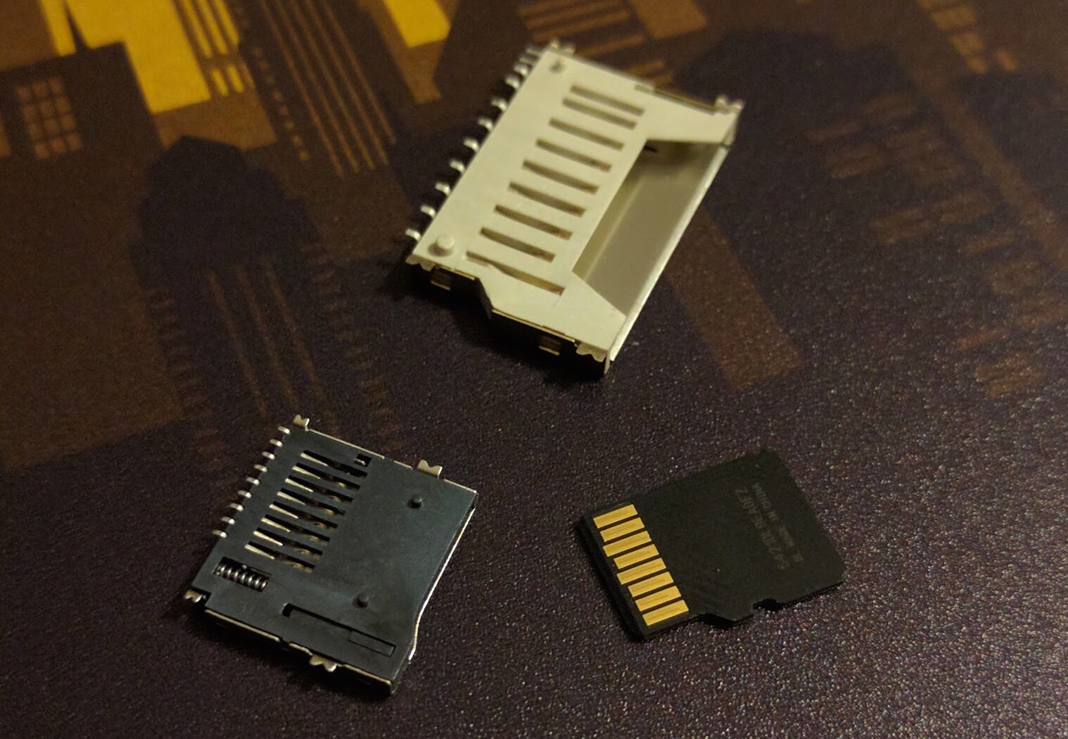
Some time ago I sourced a number of very cheap SD card sockets from China for a hobby project I was working on. Sadly, when it came to PCB design, I couldn’t find the footprints for this particular socket anywhere - the part being a proprietary invention of the factory rather than a cheap knockoff of a reputable brand like Amphenol or Molex for which drawings are readily available off of snapeda.com.
Turns out, this is a problem with many, many parts - there are no CAD drawings to be found anywhere, and the only way to really fit the part onto a board is to measure the part and draw everything yourself - a tedious manual process, but with a few tools, any part can be precisely drawn and transferred onto the board.
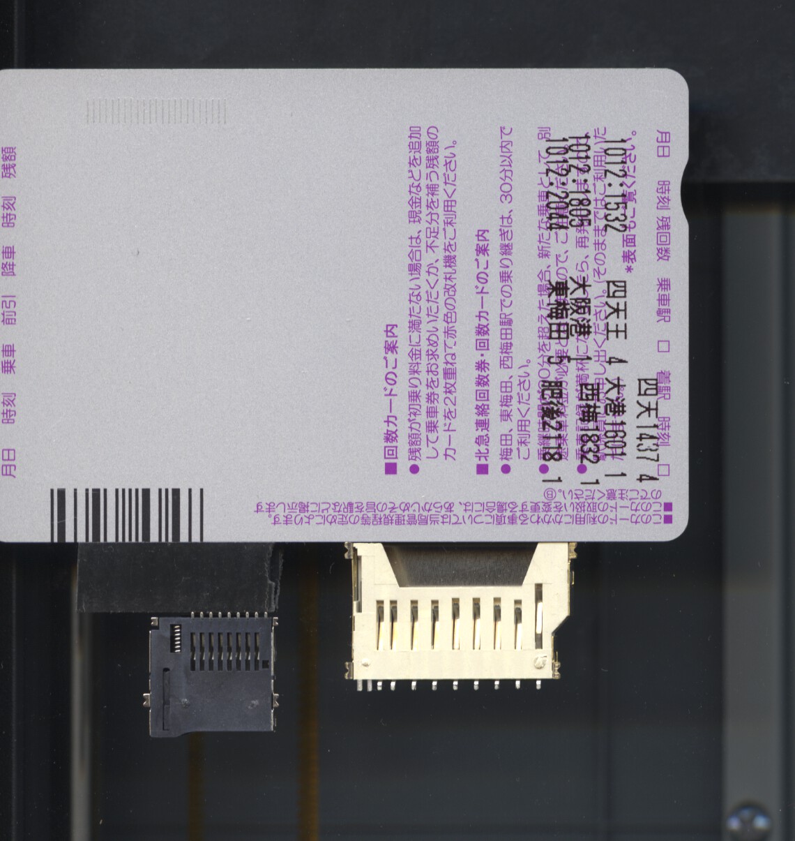
Step one - Scan the part using a flatbed scanner
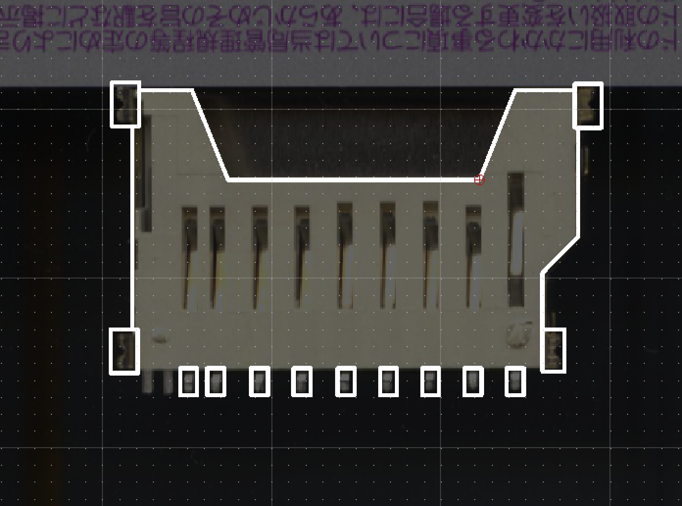
In the absence of other tools, one can use any flatbed scanner to reproduce the measurements required to draw a part. At 300dpi, a scan will yield a sufficient measurement on most, if not all parts. One key thing to remember is to ensure that each part is aligned with the edge of the scanner - I’ve managed to accomplish this, using a public transport card I’ve found in my drawer. Simply place the card (or any other rectangular item) next to the edge, and make sure it touches it and is aligned with it, then - align your parts with the edges of the card. The alternative is to use the edges of the scanner to align the parts, but I’ve found that to be unreliable.
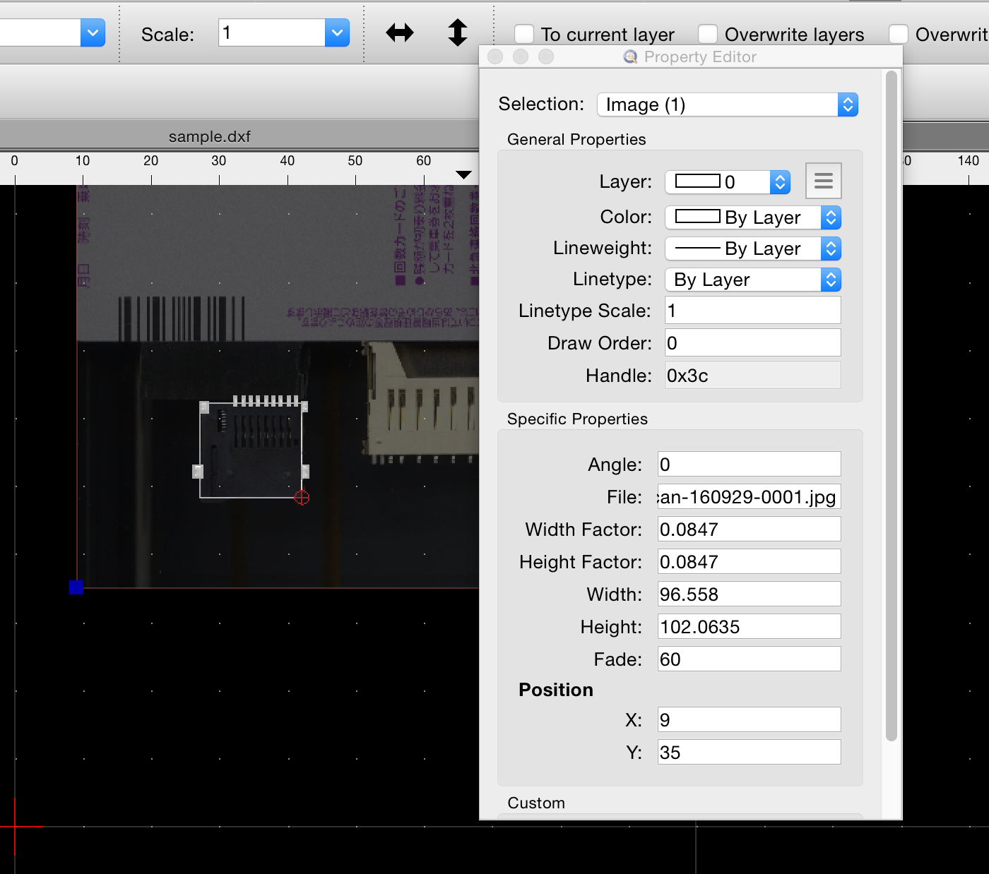
Step two - Open your CAD package and import the bitmap
Fire up your favorite CAD package (QCAD is my choice), and import the bitmap. Ensure that it is scaled properly - in my case (a 300 dpi) scan, the width/height factor turned out to be 0.0847 (300 dpi is 11.811 dots/mm, and 1/11.811 = 0.08466683600033867).
Step three - draw your part
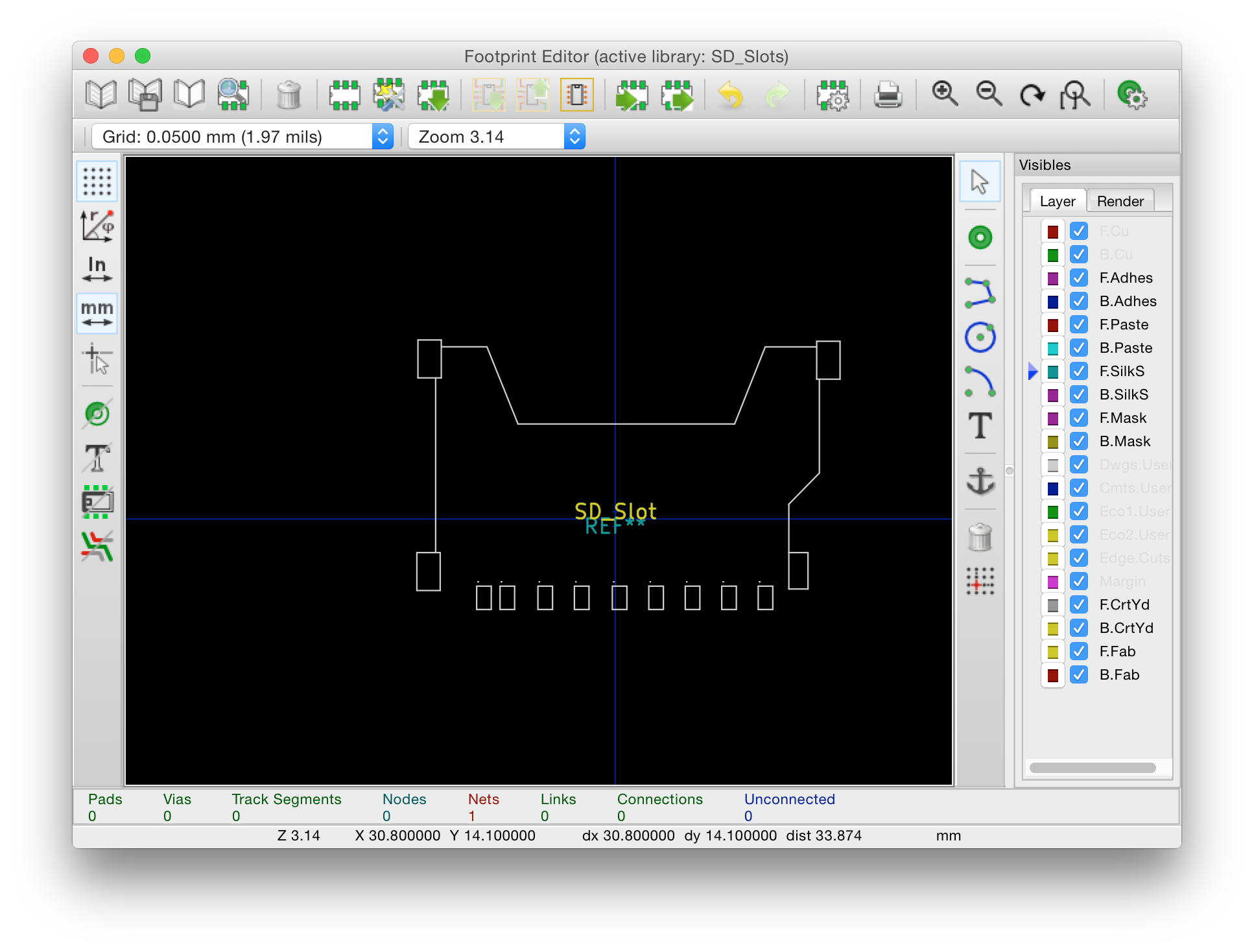
Next, select the rectangle tool, and draw an outline over your first pad. There are a number of tools in QCAD that make it easy to place copies of a pad equidistantly - use them, or place everything by hand.
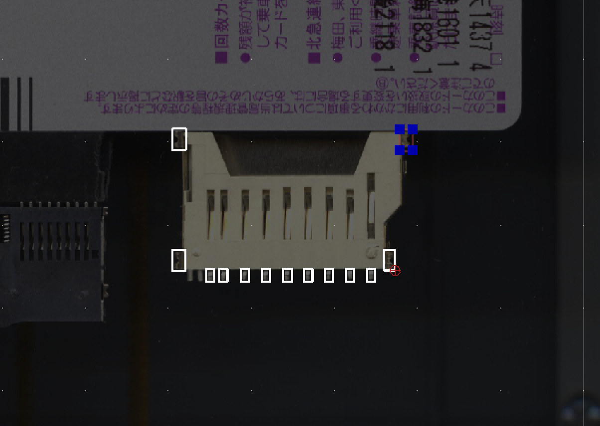
Next, if you like, you can draw the outline of the part as well - this is useful for when you will want to transfer it into KiCad’s footprint editor and place them on the silkscreen layer.
Step four - export as DXF and import into KiCad
Assuming you have saved your drawing as DXF, fire up KiCad, open the footprint editor, and select the library you wish to place your future footprint in. Click on the “New footprint” icon, and select a name. Select File | Import DXF File, select your file, and then select a layer you wish to import your drawing into - I’ve used ‘Dwgs.User’. The drawing we import will be used to trace over, and will be removed later.
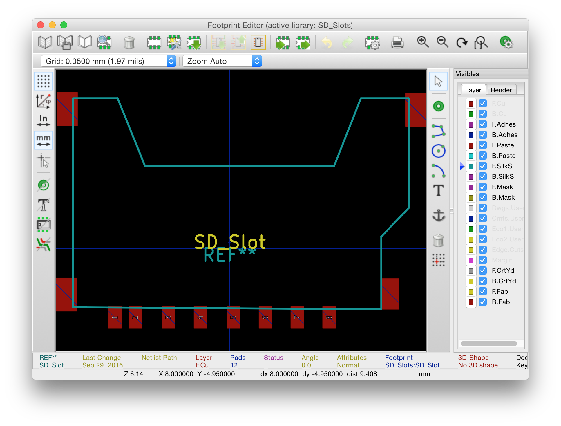
Step five - draw your pads on top of the drawing you imported
Select the pad placement tool, and place your first pad - click in the middle of a pad on the imported drawing and a modal will pop up, prompting you to select the kind of pad, its name, dimensions, etc. In my case, I’ve selected a rectangular SMD pad, entered the right dimensions through trial and error, and ended up with my first pad.
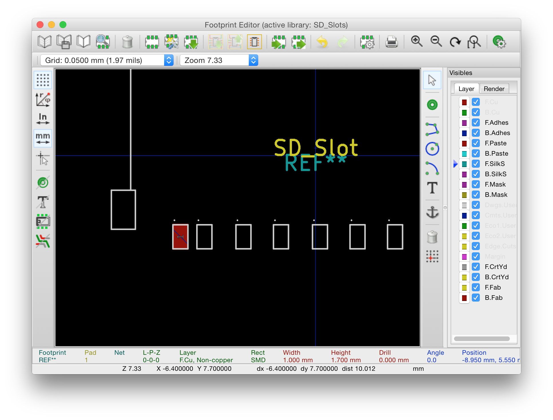
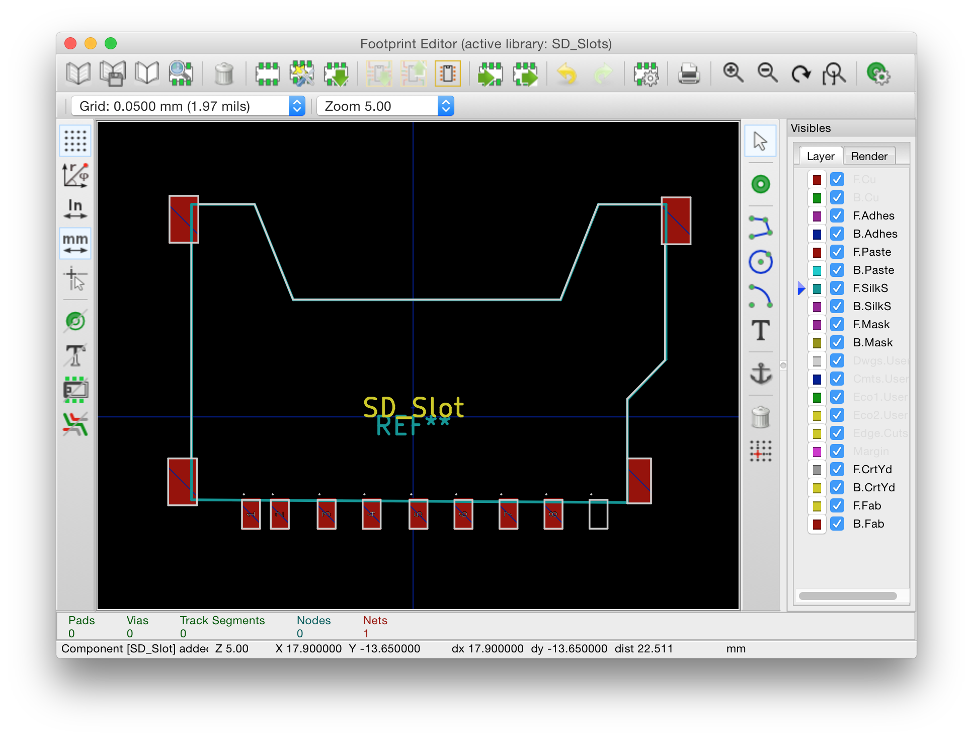
When you’re finished drawing pads, you can proceed to the silkscreen layers to draw the outline of your part.
Step six - remove the imported drawing
Since we no longer need it for anything - you can remove the drawing you imported from QCAD. There’s no good way to remove all line segments using the footprint editor, other than manually removing them by hand. Fortunately, kicad_mod files are just what appears to be LISP code - meaning you can simply remove all lines with ‘Dwgs.User’ in them. Edit them out and save the file - you’ll need to restart KiCad for these changes to be refreshed within the footprint editor.
Step seven - you’re done
Assuming you have arrived here - your part is ready to be associated with components and placed on the PCB. This process took me approximately 15 minutes from start to finish, including scanning.
